Intel has released its Penryn processor fabricated using 45-nanometer process technology recently. Following the trend, IBM has also announced the roll out plan for its first 45-nanometer process technology CBE (Cell Broadband Engine) during recent ISSCC (International Solid State Circuits Conference). The CBE is a microprocessor architecture co-developed by IBM, Toshiba and Sony targeted to fill the gap between conventional and more specialized high end processors. The new process technology is believed to be able to yield smaller parts with more efficient thermal dissipation and more importantly the BOM (Bill of Material) cost reduction in this competitive market place.
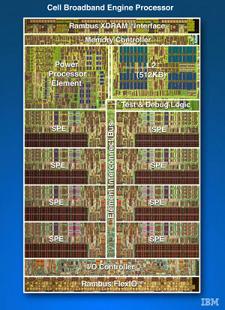
According to analysts, the die shrinks from current 65-nanometer down to 45-nanometer can save a significant 40 percent in terms of power consumption and additional 34 percent on BOM cost. Both this are crucial to compete over its rivals such as Microsoft and Nintendo in the gaming segment. Besides Sony’s PS3, there are other applications like IBM’s Industrial server and Toshiba’s mobile graphics that will able to benefit from the die shrinking process.
IBM will start fabricating new CBE processors beginning of this month. However, no firm date on the actual implementation in end products yet. Anyway, we should expect a cheaper version of PS3 with smaller form factor and better thermal efficiency in near future.
 Tip and Trick
- How To Download HBO Shows On iPhone, iPad Through Apple TV App
- Windows 10 Insider Preview Build 19025 (20H1) for PC Official Available for Insiders in Fast Ring – Here’s What’s News, Fixes, and Enhancement Changelog
- Kaspersky Total Security 2020 Free Download With License Serial Key
- Steganos Privacy Suite 19 Free Download With Genuine License Key
- Zemana AntiMalware Premium Free Download For Limited Time