Previously we talked about the new IBM’s CBE fabricated using 45-nanometer process technology. The migration effort from 65-nanometer to 45-nanometer is not simple as it involves huge design experience and high technology manufacturing process to achieve this. With the design tool introduced by IBM, the design complexity can be further reduced with the assistance of this advanced layout tool which automates some of the transition process.
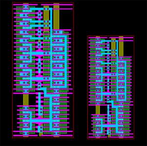
Known as MASH (Migration Assistant Shape Handler), the layout tool is smart enough to shrink basic Flip-Flop design to be suitable for 45-nanometer manufacturing automatically. Although some parts may still need manual checking and correction by layout designers, but the tool can effectively reduce the design effort and help speeding up the whole development cycle. That is not all, the tool can replace as much of the dynamic circuitry with CMOS static circuitry as possible which helps to improve the thermal efficiency by 40 percent as compared to silicon manufactured using 65-nanometer process technology.
This is one of the good examples of utilizing intelligent software tool to simplify design process. And the benefits of this transition is not only limited to silicon manufacturers but also to all consumers as a whole.
 Tip and Trick
- How To Download HBO Shows On iPhone, iPad Through Apple TV App
- Windows 10 Insider Preview Build 19025 (20H1) for PC Official Available for Insiders in Fast Ring – Here’s What’s News, Fixes, and Enhancement Changelog
- Kaspersky Total Security 2020 Free Download With License Serial Key
- Steganos Privacy Suite 19 Free Download With Genuine License Key
- Zemana AntiMalware Premium Free Download For Limited Time